Focus on Precision Cleaning
-
 E-Mail
 -
 WhatsApp/WeChat
 -
 Phone
Phone
In the fast-paced world of electronics manufacturing, the smallest contamination can lead to major reliability issues. For PCB Manufacturing Engineers, Quality Managers, and Process Engineers, maintaining surface cleanliness is critical to achieving high yield rates and preventing costly field failures.
Microscopic residues — from drilling debris, flux, copper particles, or handling oils — can cause delamination, signal loss, or even short circuits. Unfortunately, traditional PCB cleaning methods such as manual brushing or spray rinsing often fail to reach blind vias, under BGAs, or densely packed microstructures.

This is where industrial ultrasonic cleaning technology becomes indispensable — providing a precise, repeatable, and non-destructive cleaning solution that ensures consistent PCB yield improvement and long-term reliability.
Conventional cleaning methods rely on chemical action and macroscopic fluid movement. While they can remove gross contaminants, they struggle with sub-surface debris in micro-vias, under components, and within densely packed traces. Incomplete cleaning can lead to a host of failures:
In a world where miniaturization and HDI (High-Density Interconnect) designs dominate, these issues can quickly compound into production-wide reliability problems.
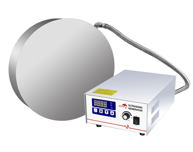
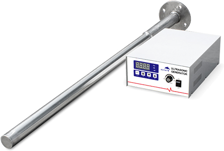
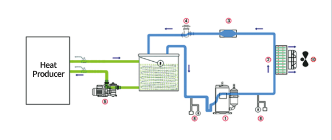
Ultrasonic cleaning harnesses the power of acoustics. A generator creates high-frequency electrical signals, which a transducer converts into mechanical vibrations in a cleaning fluid. This process generates millions of microscopic bubbles in a phenomenon known as cavitation.
These bubbles form and collapse with immense energy, creating microscopic scrubbing jets that aggressively dislodge contaminants from every surface, including blind vias, crevices, and under low-clearance components. This ensures a level of cleanliness that manual or spray methods simply cannot achieve.

Key benefits:
Implementing ultrasonic cleaning at strategic points in the production line is crucial for preventing defect propagation.
Drilling and routing leave behind epoxy smear and debris in vias. Ultrasonic cleaning effectively removes this drilling debris, ensuring a clean, conductive surface for subsequent copper plating and preventing via failures.
After etching, micro-roughness and residual copper particles ("floaters") can remain. Ultrasonic cleaning removes these particles, preventing short circuits and improving the definition of fine-line traces.
This is one of the most critical applications. Flux removal is essential to prevent corrosion and current leakage. Ultrasonic energy effortlessly dissolves and removes both water-soluble and no-clean flux residues from under BGAs, QFNs, and other complex components.
Any organic or particulate contamination on the copper surface will lead to poor adhesion of the final finish. Ultrasonic cleaning ensures a pristine surface, resulting in a uniform, high-quality finish that is critical for solderability and shelf life.
Cleaning inner layers before lamination removes oxides and handling contaminants, promoting superior bond strength and preventing delamination during thermal cycles.
HDI board cleaning presents unique challenges. With higher aspect ratio vias, finer traces, and increased density, the risk of trapped contaminants is magnified. Ultrasonic systems for HDI must be precisely calibrated. Lower frequencies (e.g., 25-40 kHz) provide more aggressive cleaning for stubborn debris, while higher frequencies (e.g., 80-130 kHz) offer gentler, more precise cleaning for delicate micro-structures without risk of erosion. A multi-frequency system is often ideal for facilities handling a mix of standard and advanced PCBs.

With continuous technological improvements and automation integration, industrial ultrasonic cleaning machines are helping manufacturers achieve cleaner, more efficient, and environmentally sustainable production worldwide. Selecting the right ultrasonic cleaning system is paramount to achieving the desired results without causing damage. Consider these factors:
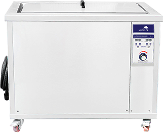
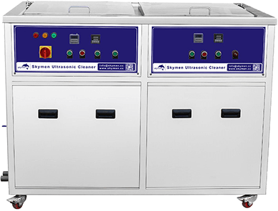
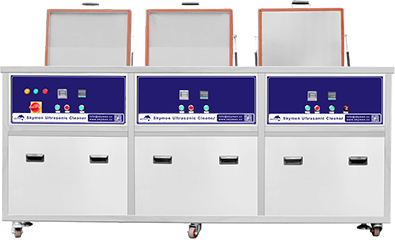
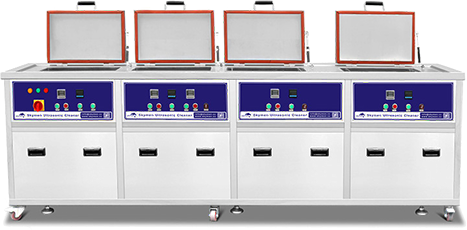
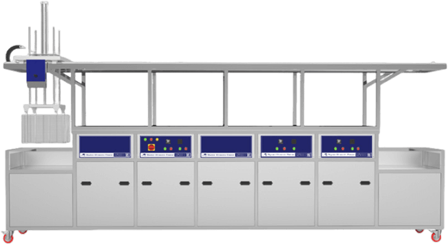
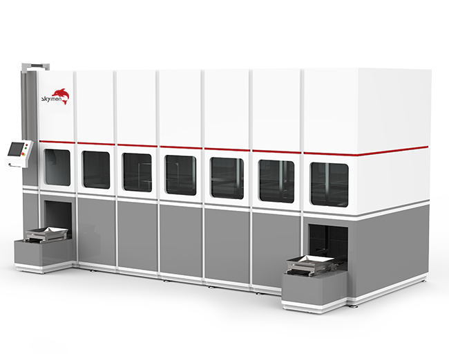
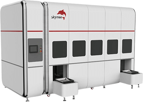
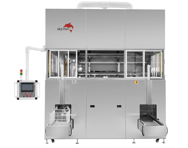
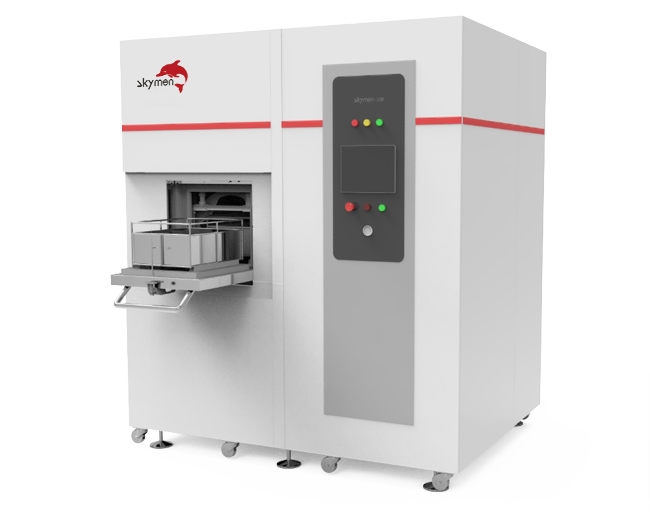
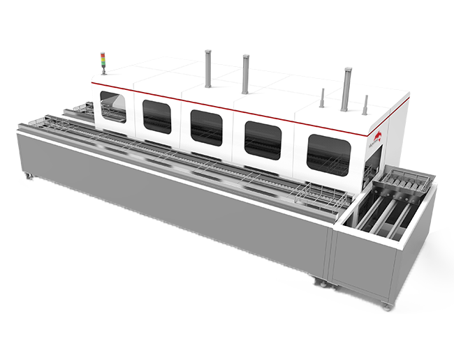
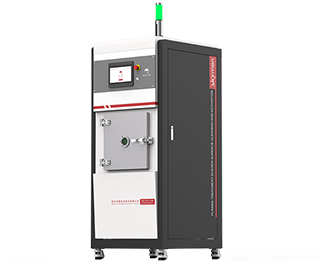
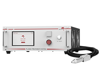
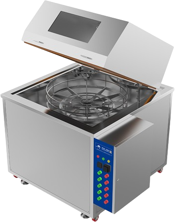
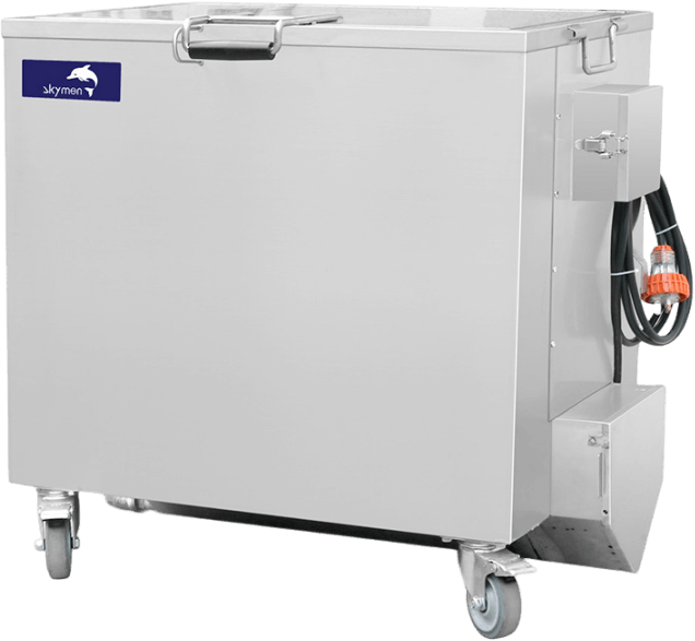
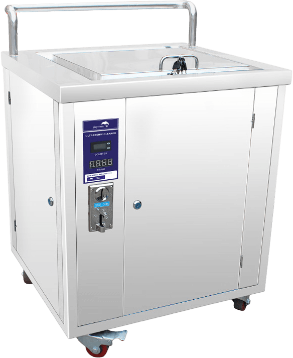
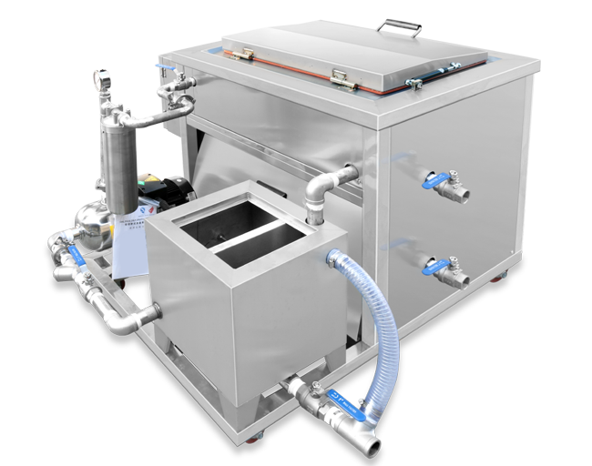
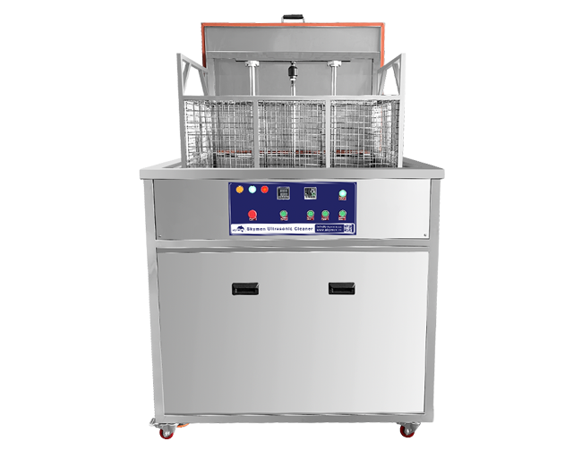
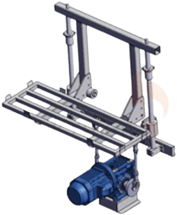
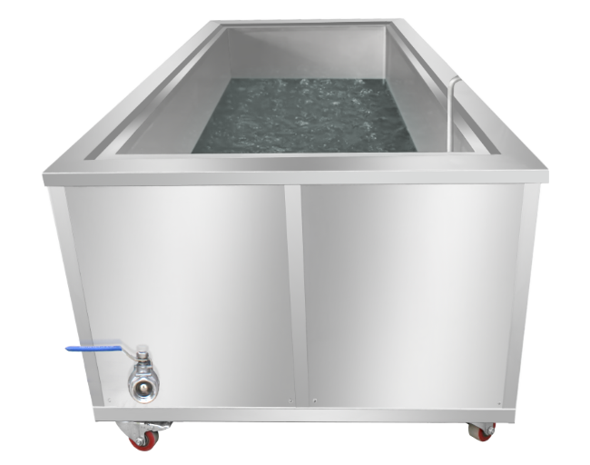
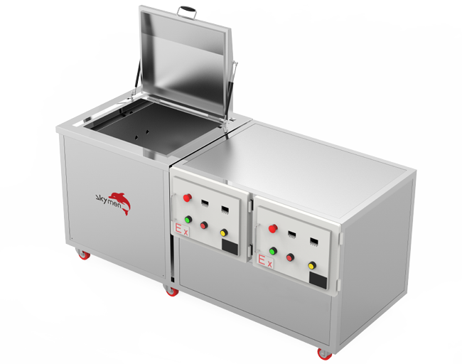
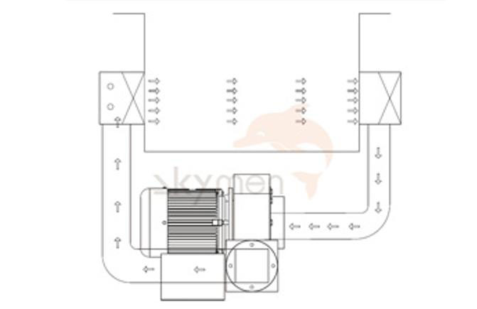
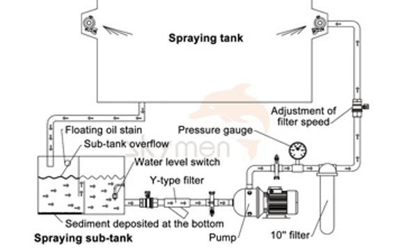
For manufacturers seeking robust and reliable solutions, Skymen addresses pain points in PCB manufacturing by offering semi-automatic ultrasonic cleaning equipment and fully automatic multi-tank cleaning lines. These equipment are compatible with robotic loading and unloading arms and seamlessly integrate with automatic production lines to improve production efficiency. Equipped with a high-precision circulating cleaning system, integrating filtration, distillation, and pure water recovery modules, they reduce wastewater discharge and comply with RoHS and IPC standards. From standard PCB cleaning to advanced HDI board cleaning, they ensure optimal yield and superior reliability.


In an industry driven by precision and performance, leaving cleanliness to chance is not an option. Ultrasonic cleaning technology is not merely a cleaning step; it is a critical quality assurance process. By systematically eliminating contaminants at every stage, manufacturers can significantly reduce field failures, improve end-product performance, and protect their bottom line through substantial PCB yield improvement. Investing in the right ultrasonic cleaning system is an investment in product quality and brand reputation.
Ready to elevate your PCB manufacturing process? Explore how advanced cleaning solutions can solve your toughest contamination challenges.